Qualcomm unveils adreno X2 GPU with enhanced architecture
Qualcomm's Adreno X2 GPU, part of the Snapdragon X2 Elite, doubles the theoretical compute throughput of its predecessor, the Adreno X1.
Qualcomm has launched the Adreno X2 GPU, which builds on the Adreno X1 architecture but significantly enhances performance through an expanded shader processor (SP) layout and higher clock speeds. Each Adreno X2 SP consists of two Micro Shader Processor Texture Processors (uSPTPs), each with 128 FP32 lanes and 128 KB of register file capacity. The Adreno X2 features eight SPs grouped into four slices, compared to six SPs in three slices in Adreno X1, with clock speeds increasing from 1.5 GHz to 1.85 GHz. This upgrade results in nearly double the theoretical compute throughput, though the GPU requires more parallelism to reach its maximum performance.
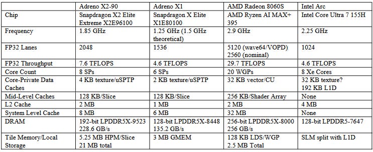
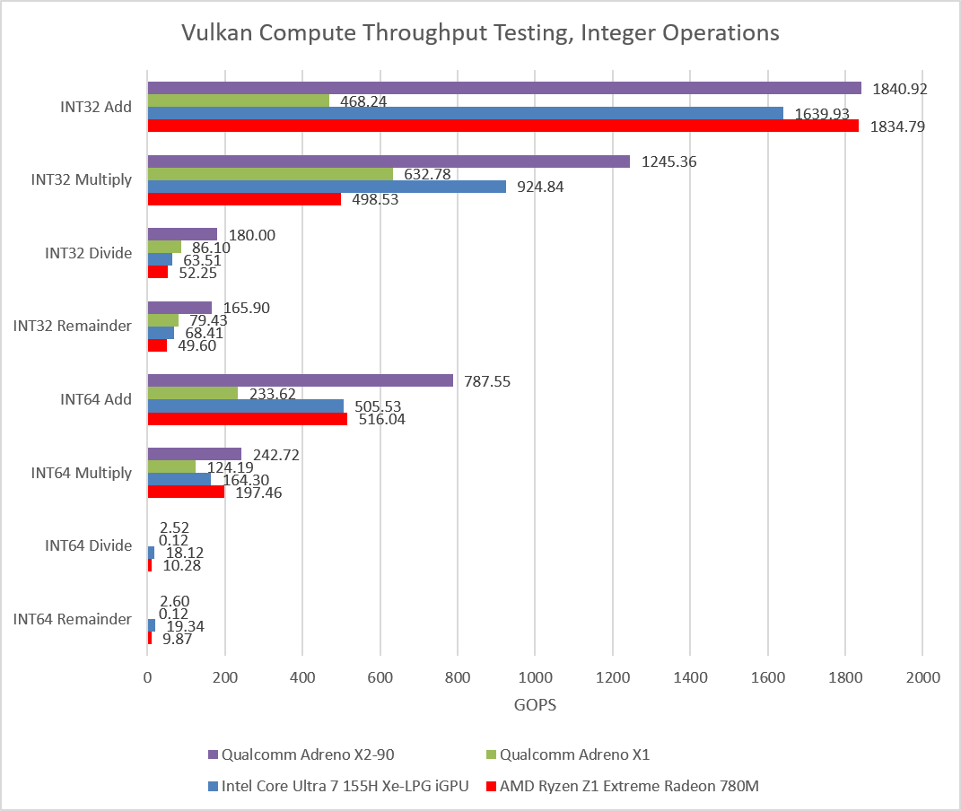
The Adreno X2 architecture includes improvements in integer performance, with INT32 operations executing at full rate, a significant enhancement over Adreno X1 where basic integer operations executed at less than half rate. Despite these improvements, the Adreno X2 still lacks hardware fused multiply-add (FMA) capability, leading to poor throughput when using OpenCL's fma() function. The Adreno X2 also has a more robust memory hierarchy, with larger cache sizes and increased bandwidth to handle the higher throughput demands of the enhanced architecture. However, the texture cache remains small at 4 KB per uSPTP, impacting performance compared to competitors like AMD's RDNA3.5.
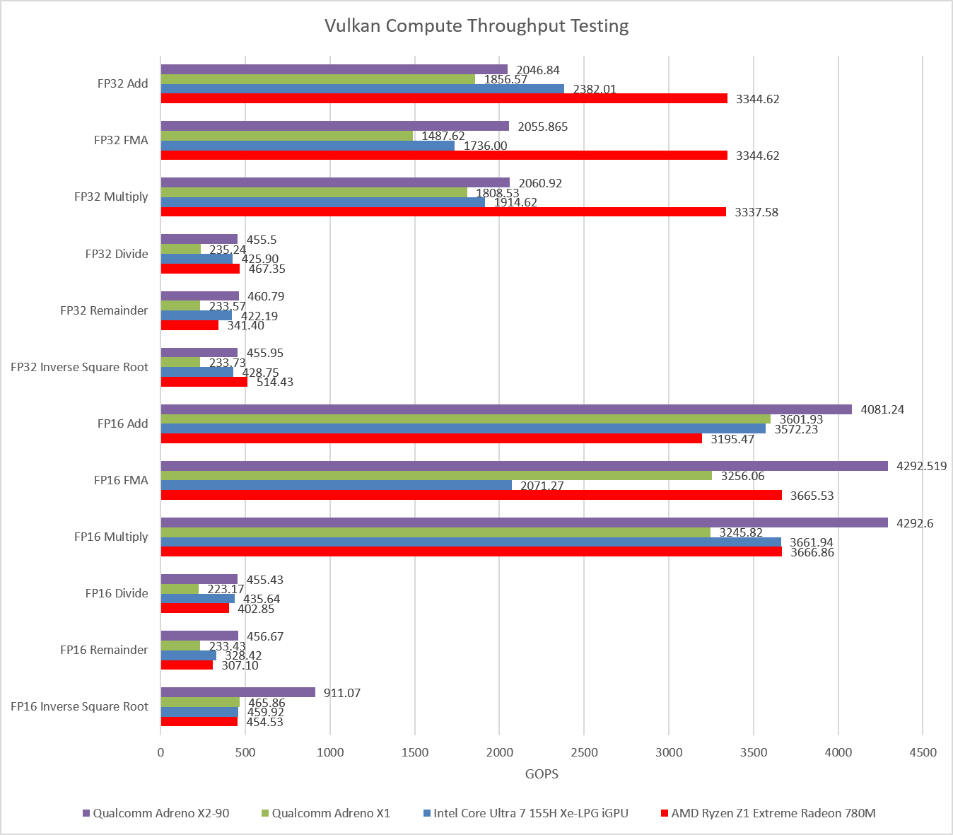
Compared to the Adreno X1, the Adreno X2 sees a significant boost in theoretical compute throughput, thanks to the addition of two more SPs and a 23% increase in clock speed. This change also necessitates a more powerful memory subsystem, with larger cache sizes and higher bandwidth to support the increased computational demands. The Adreno X2's architecture is designed to emphasize high throughput for basic FP32 and FP16 operations, with improvements in integer performance, though it still lacks FP64 support. The enhanced architecture aims to provide better graphics performance in ultraportable devices, aligning with Qualcomm's push for more powerful integrated GPUs in laptops.
The article does not provide detailed performance benchmarks or comparisons against specific competitor models, such as AMD's Strix Point or Nvidia's offerings. Additionally, the exact theoretical occupancy of the Adreno X2 is not disclosed, making it challenging to fully evaluate the performance benefits of the enhanced architecture relative to its predecessor. The source also lacks specific details on the Adreno X2's instruction cache capacity and the exact number of wave slots per uSPTP partition, leaving some aspects of the architecture unconfirmed.
Moving forward, it will be crucial to see how the Adreno X2 performs in real-world applications and benchmarks, particularly in comparison to other high-end iGPUs from AMD and Intel. Analysts and reviewers will be watching for performance metrics and power efficiency to determine the Adreno X2's position in the competitive integrated GPU market. The architectural enhancements, coupled with the increased memory bandwidth and cache sizes, suggest potential for significant improvements in graphics and compute performance, but the extent of these benefits will be clearer with more detailed benchmark data.
The Adreno X2's architecture demonstrates Qualcomm's commitment to enhancing integrated GPU performance, with notable improvements in shader processor count, clock speeds, and memory hierarchy. However, the lack of detailed performance benchmarks and specific architectural details leaves room for further evaluation.
8 SPs grouped into 4 slices · 1.85 GHz clock speed · 4 KB texture cache per uSPTP · 128 KB register file per uSPTP
After SemiAnalysis-adjacent HN. We did not report this. The pictures, if any, are theirs.