Qualcomm validates two-layer HBC ahead of 2027 Dragonfly AI250 sampling
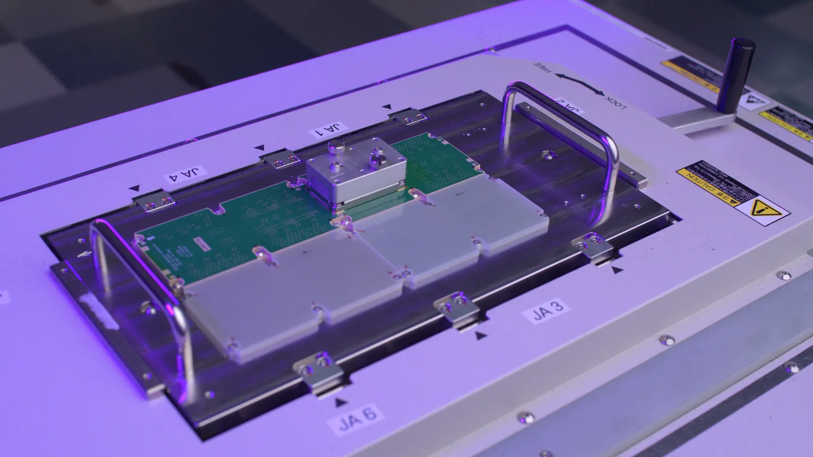
A two-layer HBC stack cleared Qualcomm's initial validation ahead of 2027 Dragonfly AI250 sampling.
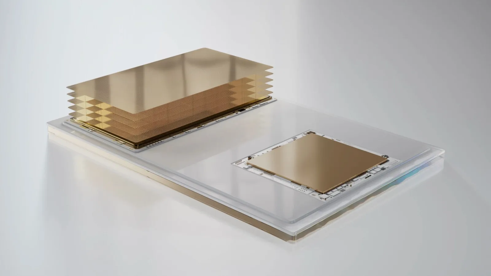
| HBC | |
|---|---|
| early sample DRAM layers | 2 |
| shipping DRAM layers | 4 |
| bandwidth-per-watt vs HBM4 | more than five-times |
| bandwidth vs external LPDDR5X | 18x higher |
| initial projection vs HBM4 | 6x |
| first product | Dragonfly AI250 |
The two-layer test stack posted more than five-times HBM4 bandwidth-per-watt and 18x external LPDDR5X bandwidth.
The early result did not meet a 6x projection, and ServeTheHome frames it as a lab test rather than a product spec.
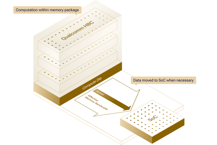
The 4-layer shipping stack still lacks measured absolute bandwidth, thermal margin, and confirmation that the 5x efficiency survives packaging.
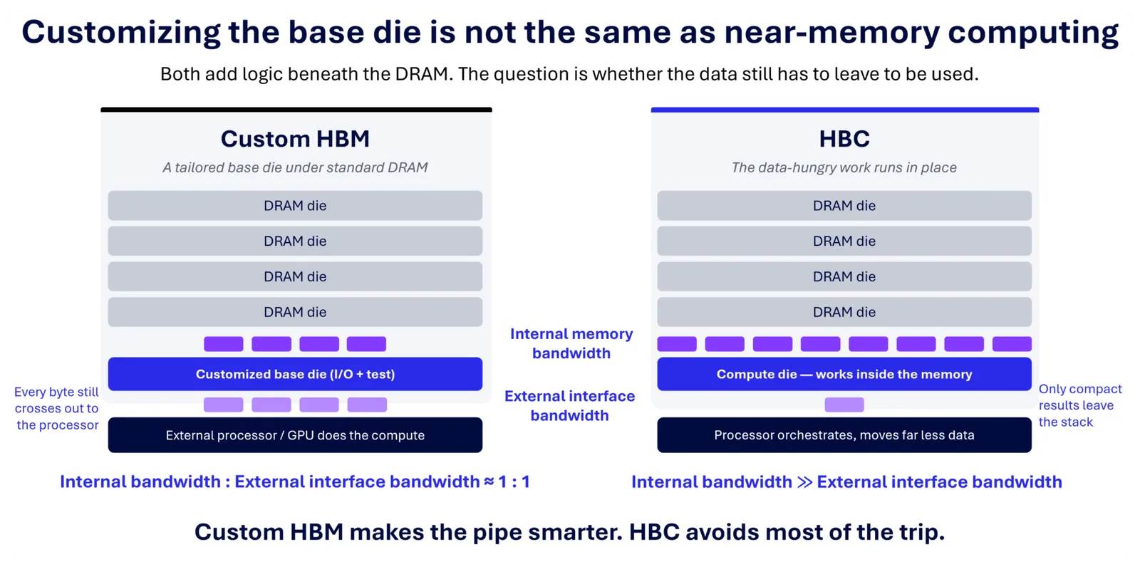
TSV bonding and heat under an active base die remain the open constraints.
No price, full AI250 configuration, manufacturing partners, or 4-layer thermal data appears in the validation.
The takeaway is that HBC is a packaging cost lever, not a current AI250 spec.
The two-layer result validates the path, but the 4-layer shipping stack remains unproven.
After servethehome.com. We did not report this. The pictures, if any, are theirs.