Micron skips G10 and moves G11 to 400-plus layers
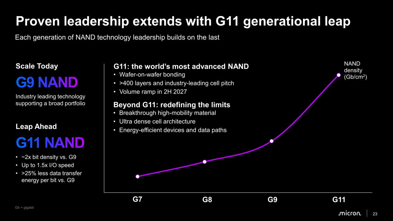
G10 is the missing number in Micron's NAND roadmap, with G11 listed at 400-plus layers and mass production in the second half of 2027.
| Micron G11 | Micron G9 | Kioxia/Sandisk BiCS10 | |
|---|---|---|---|
| layers | 400+ | 276 | 332L |
| bit density | 42 Gbit/mm² estimated | 21 Gbit/mm² | 37.6 Gbit/mm² QLC |
| interface speed | 5.4 Gbit/s estimated | 3.6 Gbit/s | 4.8 Gbit/s |
| energy per bit | >25% lower than G9 | ||
| mass production | second half 2027 |
The jump from G9's 276 layers to 400-plus is a packaging and cell-pitch bet, not a measured density win.
Micron frames wafer-on-wafer bonding and an interface up to 50 percent faster as the path to roughly double G9's bit density.
Estimated 42 Gbit/mm² for TLC and 5.4 Gbit/s interface are projections, not measured cells.
Still unmeasured are the exact layer count, confirmed TLC density, exact interface speed, exact energy per bit, and a production date beyond second half 2027.
The roadmap leaves the next generation unnamed, with only Ultra Dense cell architecture and Breakthrough high-mobility material as labels.
No price is named yet, and buyers get a roadmap claim, not a part number.
Fabs face a bonding and high-mobility material path before G12 is named.
The skip is a packaging bet, not a measured density win.
After computerbase.de. We did not report this. The pictures, if any, are theirs.