Onsemi's EPP Platform Uses Silicon Wafer for 5x Power Density
Onsemi's EPP platform replaces traditional PCB substrates with silicon wafers, promising up to 5x power density for AI chips and EVs.
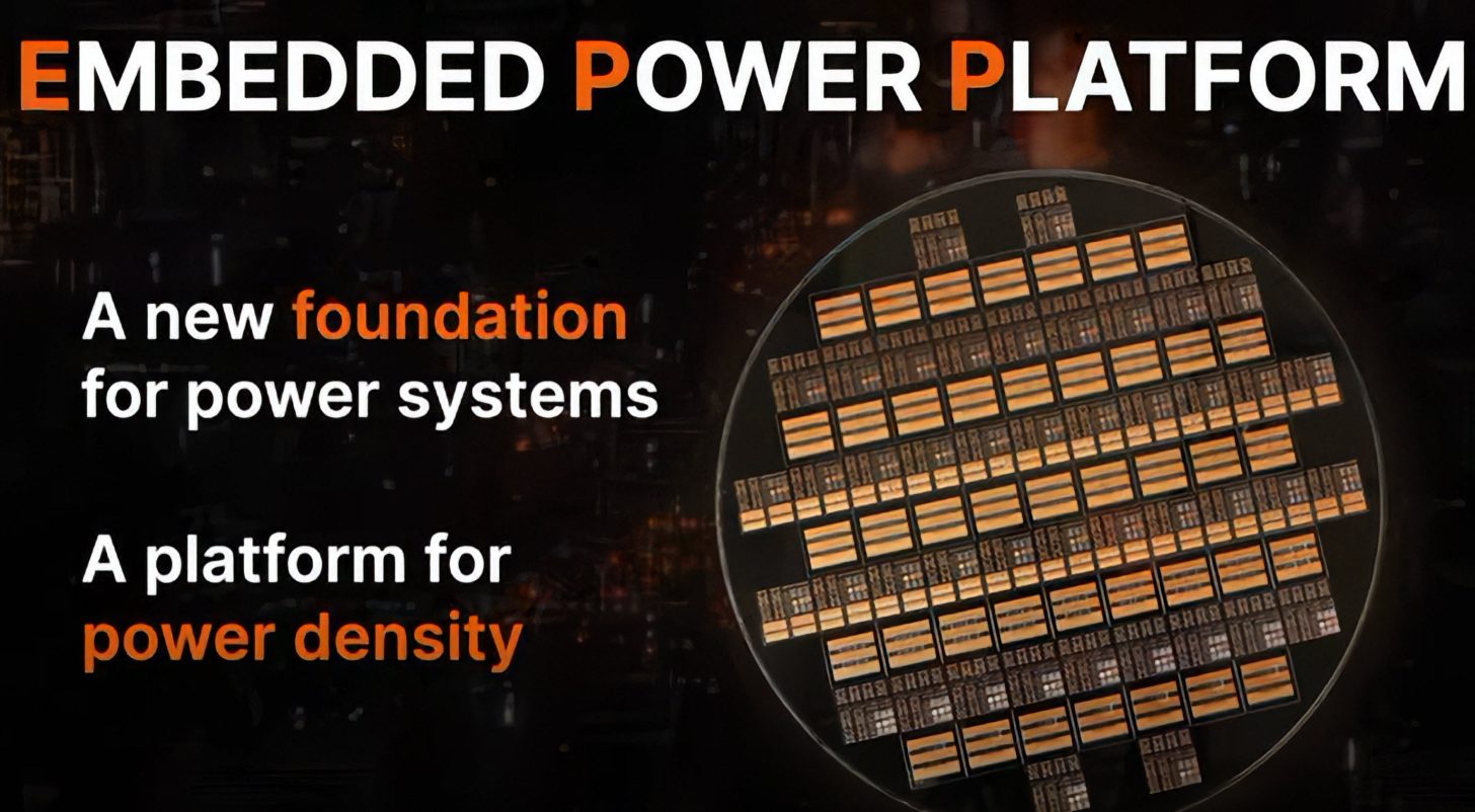
According to Wccftech Hardware, Onsemi's EPP (Embedded Power Platform) replaces traditional PCB substrates with silicon wafers, aiming for up to 5x power density in AI chips and EVs. EPP integrates silicon, silicon carbide (SiC), and gallium nitride (GaN) technologies within a wafer-level architecture, embedding power systems directly into the package substrate. This approach reduces power losses and improves thermal performance compared to conventional methods. EPP is designed to address efficiency losses and thermal limitations in EV traction inverters, enabling smaller, lighter, and more efficient designs.
The technology is also targeted at AI infrastructure, offering compact power systems and improved thermal management.
Desk take
Onsemi's EPP leverages advanced packaging to enhance power efficiency and density. While promising, its widespread adoption hinges on cost and manufacturing feasibility.
EPP's wafer-level integration could redefine semiconductor packaging, enabling higher performance and efficiency in power-hungry applications.
Source dispatch
Onsemi's EPP (Embedded Power Platform) aims to utilize silicon wafers to enable more efficient and power-dense chips. As Power Demands Grow, Onsemi Is Working on Its EPP Solution To Make Semiconductors More Efficient & Denser Currently, power modules within a chip are placed within the PCB (Printed Circuit Board), but as more advanced packaging solutions are being developed, we are seeing the embedding of power systems within the package substrate. Intel's EMIB is one example where the TSVs route power to the chip around the embedded package, and EMIB-T takes it one step further by routing power through the embedded […]