Anthropic's reported Samsung accelerator is a pilot, not a confirmed fab deal
Anthropic's reported accelerator would run at 4,000 TOPS at INT8 and 1,300 W TDP, but Samsung has not confirmed the foundry agreement.
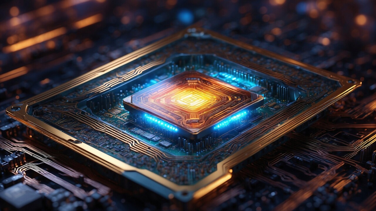
Reported specs put the accelerator at 4,000 TOPS at INT8 and 1,300 W TDP, with 192 or 288 GB of HBM3E as memory options. The ComputerBase headline says "soll bei Samsung gefertigt werden", but the article body says the agreement is not officially confirmed. Trust the article body; the number that decides it is 200,000 chips.
This is a pilot, not volume. A 2 nm SF2 node and a 1,300 W power figure require Samsung to prove SF2 readiness, HBM integration, and cooling before Anthropic can scale beyond a pilot. The buyer is constrained by unverified yield, packaging, and rack power, while the fab is constrained by the need to show a workable 2 nm flow.
Packaging also leaves the HBM path uncertain. Samsung could use I-Cube 2.5D packaging, or the 2.1D Packaging Alliance work with Qualcomm might enter the design, but the article does not settle that choice. For a 1,300 W part, the bridge between die, HBM, and board determines whether the power budget stays usable in a rack.
Missing are the tape-out date, production start, SKU, selected HBM capacity, and packaging selection. It also does not show whether Taylor capacity or Korea SF2 will serve the first run. Without those items, the 4,000 TOPS figure remains a target, not a measured silicon result in a real rack.
The 200,000-chip first stage makes this a feasibility run, not a volume commitment. Samsung must prove SF2 yield, HBM integration, and cooling before Anthropic can treat the 4,000 TOPS figure as a production target.
The page leaves out the tape-out date, production start, SKU, selected HBM capacity, and packaging selection.
The 200,000-chip first stage is a pilot gate. SF2 yield, HBM3E integration, and 1,300 W cooling must be demonstrated before the 4,000 TOPS INT8 target becomes a production constraint.
4,000 TOPS at INT8 · 1,300 W TDP · 192 GB HBM3E · 288 GB HBM3E · 2 nm SF2 node · 200,000 chips in the first production stage
After computerbase.de. We did not report this. The pictures, if any, are theirs.