Samsung HBM4E qualification claim leaves volumes and production date open
Samsung's 12-high HBM4E stack is rated at 48 GB and up to 3.6 TB/s at 14 Gbit/s per pin, while qualification at Nvidia remains unconfirmed.
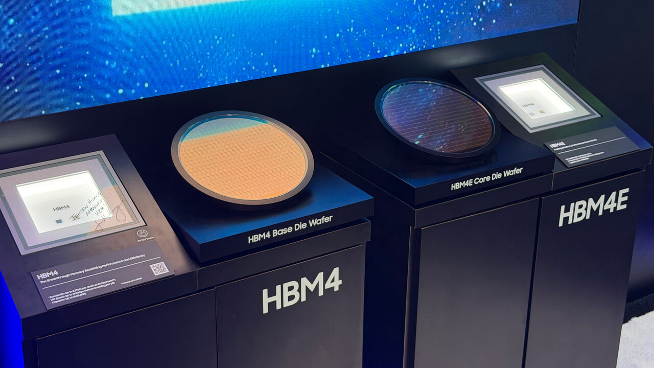
Samsung's 12-layer HBM4E stack is said to have passed qualification tests at Nvidia and several large hyperscalers. ComputerBase page has no figure, so the frame is a stack rating, not a measured platform. Stack capacity is 48 GB, and Samsung rates it at up to 3.6 TB/s at 14 Gbit/s per pin, with about 4.0 TB/s at 16 Gbit/s.
Meaningful move is the qualification claim, not the bandwidth number. It moves Samsung from sample supplier to a tested candidate, but it does not prove that Nvidia has placed an order, set a delivery volume, or fixed a mass-production date. For the buyer, the constraint is still adoption: the stack must fit Nvidia's schedule, and for the fab, the 1c DRAM and 4 nm logic die are already known from HBM4, so no new process step is shown.
Samples went out at the end of May, and the reported tests closed at the end of September. That sequence matters because Samsung had earlier trouble with HBM3e and had to redesign. Page also notes SK Hynix shipped HBM4E samples three weeks after Samsung, and that Samsung began HBM4 mass production in early 2026.
Volumes, contract values, production start, thermal margin, yield, and the actual pin rate in a finished system are not in the document. The 3.6 TB/s figure remains a stack number, not a platform guarantee. SK Hynix and Micron remain in the race, and the buyer still waits on Nvidia's adoption schedule.
The qualification claim changes Samsung's position from unverified sample to tested candidate, but it does not create a supply line. The buyer is still constrained by Nvidia's adoption schedule, and the fab side adds no new process step.
Volumes, contract values, production start, thermal margin, yield, and actual system pin rate are not measured.
Qualification is a buyer-side gate, not a production commitment. The 1c DRAM and 4 nm logic die are already HBM4 nodes, so the document proves test passage, not yield, thermal margin, or system pin rate.
12-layer HBM4E stack · 48 GB per stack · 14 Gbit/s per pin · 3.6 TB/s at 14 Gbit/s · 16 Gbit/s per pin · 4.0 TB/s at 16 Gbit/s
After computerbase.de. We did not report this. The pictures, if any, are theirs. Also filed by TechPowerUp.