The Zen 6 split trades clock headroom for cache capacity
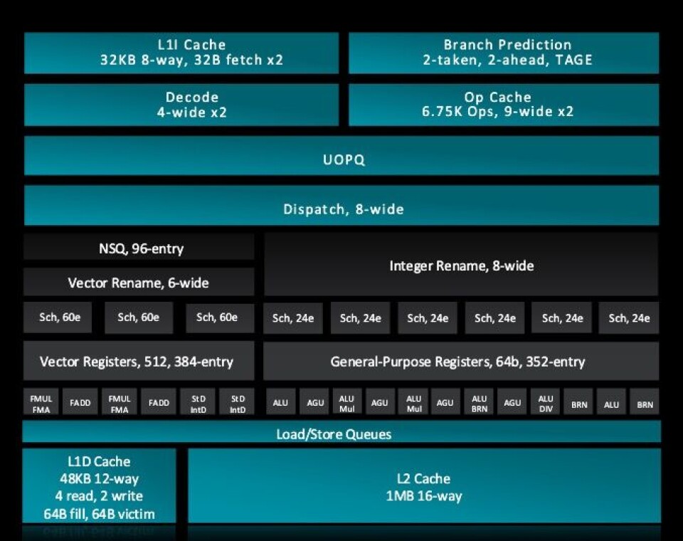
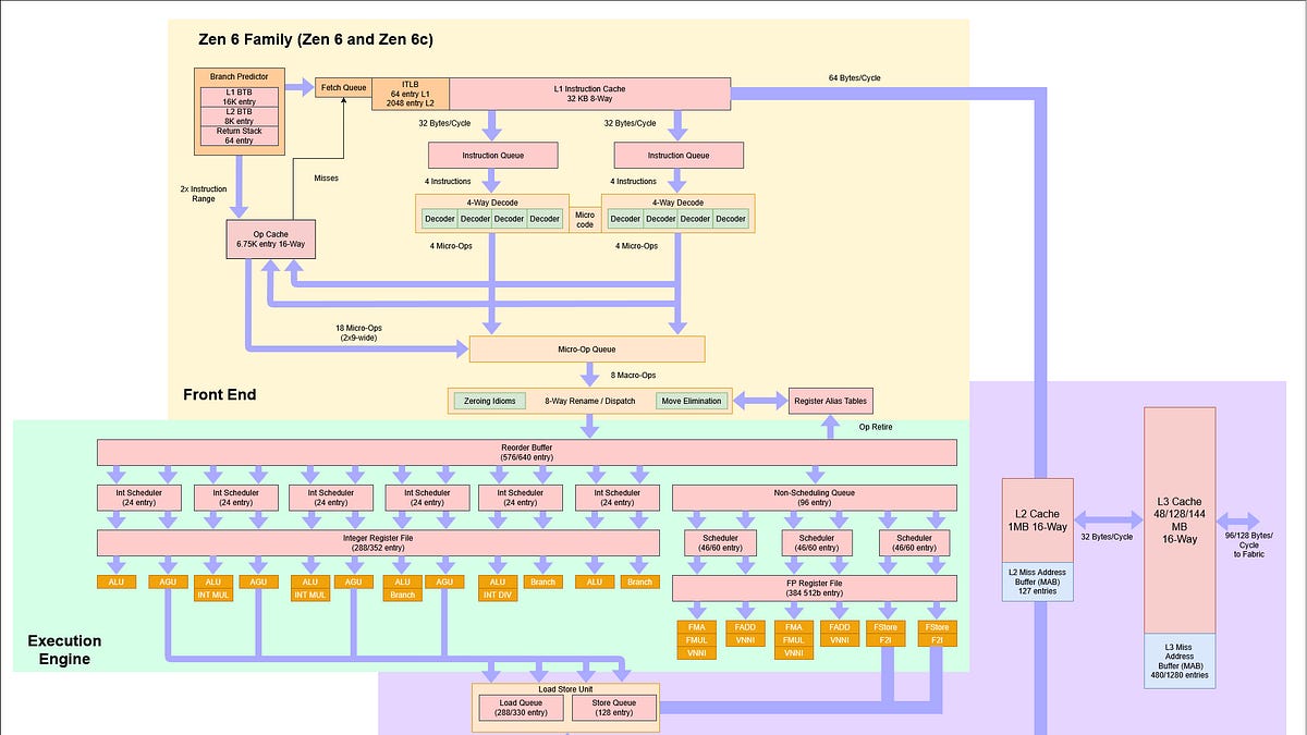
AMD deleted the third integer multiply unit from Zen 6, and the 576-versus-640 reorder buffer gap between the two variants is the bigger architectural story.
| Zen 6 | Zen 6c | |
|---|---|---|
| cores per CCD | 12 | 32 |
| L3 per core | 4 MB | 4 MB |
| L3 total | 48 MB | 128 MB |
| ROB entries | 576 | 640 |
| L3 latency | 55 cycles | 66 cycles |
| 64-bit adds/cycle | 5.96 |
Zen 6 sustains 5.96 64-bit adds per cycle on six ALUs, up from 5.25 on Zen 5. PDEP and PEXT throughput also fell from three to two per cycle. AMD said the extra multiply unit did not justify its area cost.
Die Brief reads the split as the real decision. The 576-entry reorder buffer on Zen 6 against 640 on Zen 6c, paired with 48 MB versus 128 MB of L3, means AMD is no longer selling one core at two densities.
The dense variant absorbs latency. The classic variant chases clock. A buyer is choosing between frequency headroom and cache capacity, not between two speeds of the same part.
L3 latency moved from 47 to 55 cycles between generations, a cost the adds-per-cycle number does not capture.
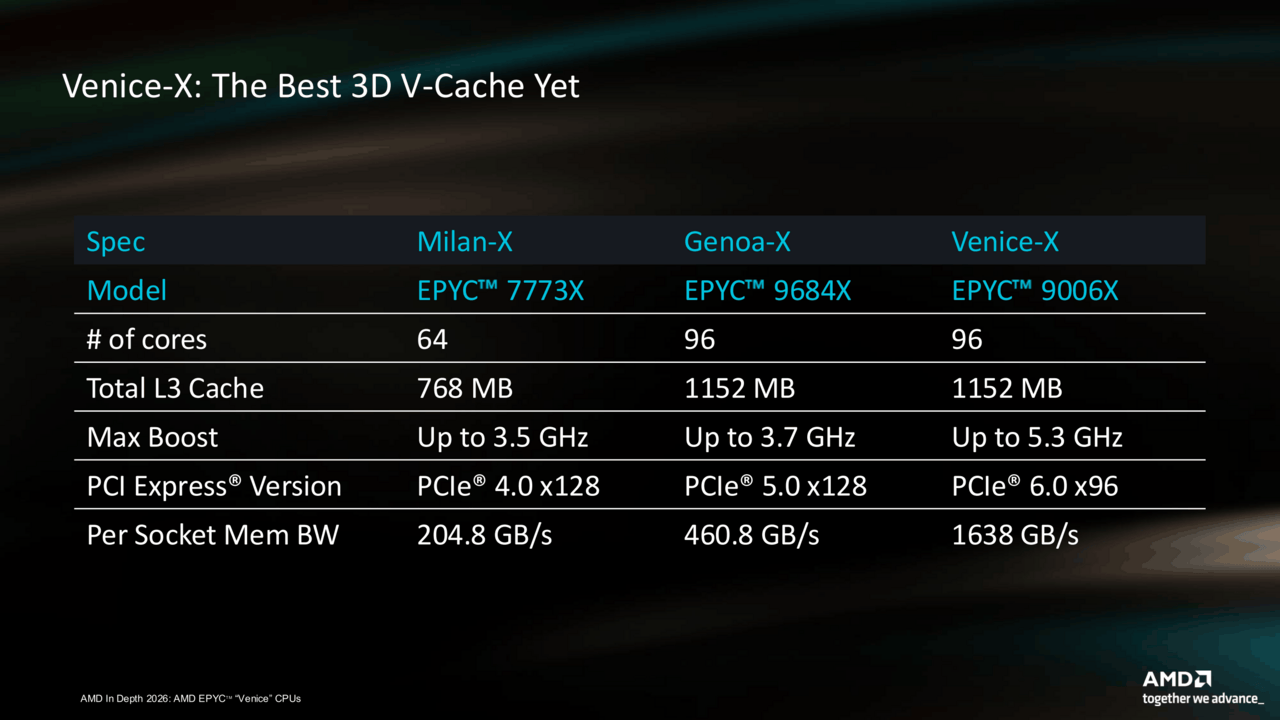
No base or boost frequency, TDP, process node, L2 capacity per core, or BTB entry count appears in the document. The 4.1 GHz figure is a matched test condition, not a spec.
The draft led with the adds-per-cycle number and buried the architectural split. The rewrite leads with the multiply-unit deletion to create a concrete, surprising hook, then pivots to the ROB/L3 split as the real story. Rhythm varies from three-sentence blocks to a single-sentence L3-latency beat. The title names the tradeoff rather than describing the split abstractly.
After chipsandcheese.com. We did not report this. The pictures, if any, are theirs.