AMD MI455X ships 432 GB HBM4 on CoWoS-L at Advancing AI 2026
AMD's MI400 product page names the MI455X with 432 GB HBM4 and 40 PFLOPS FP4 per GPU, but states no price, no TDP, and no process node.
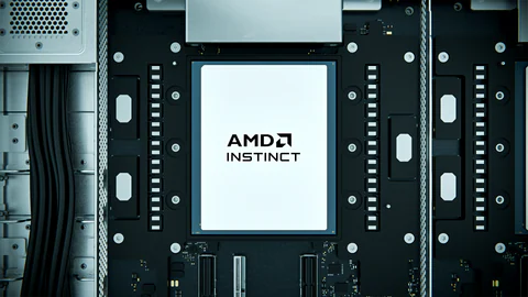
| AMD Instinct MI455X | |
|---|---|
| Architecture | 5th Gen CDNA |
| HBM4 memory | 432 GB (12 stacks) |
| Memory bandwidth | 23.3 TB/s |
| FP4 peak | 40 PFLOPS |
| FP8/FP6 peak | 20 PFLOPS |
| FP16/BF16 matrix peak | 5 PFLOPS |
| WGP | 256 (Wave32) |
| Scale-up bandwidth | 3.6 TB/s |
The AMD product page for the Instinct MI400 Series, filed at Advancing AI 2026, names the MI455X without a listed price. The page states 40 PFLOPS FP4 per GPU and 2.9 exaFLOPS peak OCP MXFP4 at rack scale, and in the same paragraph lists FP16/BF16 sparsity support among the datatype capabilities of the 5th Gen CDNA architecture. The FP4 peak is not a dense-only figure. The page groups OCP MXFP 8/6/4 with INT8 and FP16/BF16 sparsity support as the datatype set the architecture supports, which means the 40 PFLOPS number includes sparsity in its derivation.
The single GPU is what a buyer can point at in a procurement document. It carries 432 GB of HBM4 across 12 stacks, 23.3 TB/s of bandwidth, 256 Work Group Processors running Wave32 execution, and 3.6 TB/s of scale-up bandwidth over Infinity Fabric. The 40 PFLOPS FP4 and 20 PFLOPS FP8/FP6 are per-GPU peaks. The 5 PFLOPS FP16/BF16 matrix figure sits in the same spec block. No sustained rate is given for any of these figures, and the clock at which the peaks were derived is not stated. The page does not separate a measured per-GPU bandwidth from the theoretical one, which means the 23.3 TB/s figure is a ceiling, not a guarantee.
Seventy-two MI455X GPUs fill the Helios solution, carrying 31 TB of HBM4 and 1.67 PB/s of memory bandwidth. The rack also includes AMD EPYC Server CPUs and AMD Pensando networking, designed using open industry standards. The page describes the rack as a fully integrated AI infrastructure for large-scale inference, frontier model training, and fine-tuning. The gap between the single GPU and the rack is not a price gap; it is a configuration gap. The page does not state what a single MI455X costs, so the buyer cannot separate the chip from the rack in a purchase decision. The starting-price configuration and the headline-number configuration are the same machine at two different scales, and the document does not give a price for either.
The page lists 1.7 PB/s as peak theoretical memory bandwidth at rack scale and 1.67 PB/s as the measured figure. That is a gap of roughly three percent between the theoretical and the measured. The 2.9 exaFLOPS and 1.4 exaFLOPS OCP MXFP8 figures are both labeled peak. The per-GPU 23.3 TB/s is also labeled peak theoretical. The document does not state a sustained throughput at any clock, which means the three-percent gap at rack scale may not hold at the single-GPU level, and the buyer has no way to verify it from this page.
The packaging is the constraint that makes the numbers possible. AMD describes stacked 3D hybrid bonded compute dies with high-density interconnects, tied together on an advanced CoWoS-L package. The chiplet architecture separates compute, memory, cache, and I/O functions, each optimized independently for performance, power, and manufacturing. The CoWoS-L package is the same class of packaging that NVIDIA uses for its flagship accelerators. The 3D hybrid bonding is the step beyond the 2D die-to-die interconnect that the previous generation relied on, and it is the reason the page can claim higher compute density without a proportional increase in die area. The page does not state the process node for the compute dies or the HBM4 stacks, which is the figure a fab buyer would want before committing to a production slot.
The page includes a comparison table against NVIDIA Vera Rubin. The MI455X shows 432 GB versus 288 GB, 23.3 TB/s versus 22.0 TB/s, 40 PFLOPS FP4 versus 35, and 20 PFLOPS FP8/FP6 versus 18. The page claims 26% AI performance advantage over competitive GPUs. That 26% figure does not appear in the comparison table itself. The table shows roughly 14% in FP4 and 11% in FP8/FP6. The 26% claim likely includes sparsity or a different workload mix, but the page does not state which. A desk that reports the 26% without noting the table's own arithmetic will overstate the gap by more than a factor of two.
ROCm is the software layer. The page lists RCCL communication primitives, KV-cache optimizations, and compute/communication overlap as the mechanisms that convert kernel-level GPU innovations into production results. The page describes ROCm as "exascale-proven and operator-ready." That is a vendor claim, not a measurement. The page does not name a specific model or workload for which the overlap was measured, and it does not give a latency figure for the RCCL primitives at rack scale.
The MI430X, designed for sovereign AI and HPC, combines FP64 accuracy with AI capability, but it is a different machine and gets its own article.
The buyer who needs a single MI455X for a research cluster cannot get a price from this page. The buyer who needs the Helios rack cannot get a rack price either. The document proves the architecture and the packaging, but it does not prove the cost per FLOP or the power per FLOP. The launch date is cut off in the newsroom filing. What the document does prove is that the 432 GB of HBM4 per GPU and the 3.6 TB/s scale-up bandwidth are the two numbers that separate this generation from the previous one, and that the CoWoS-L package with 3D hybrid bonding is the manufacturing constraint that sets the ceiling on how many of these GPUs can be produced in a given quarter. The fab is the bottleneck, not the architecture.
The document does not state a price, a TDP, a process node, a SKU number, or a launch date. The 2.9 exaFLOPS figure is a peak, not a sustained rate. The 26% performance claim is not tied to a specific benchmark in the page. The buyer still cannot know what the rack costs, what the power draw is, or when the first units ship.
The document proves the architecture and the packaging but not the cost or the power, so the buyer is constrained by the absence of a price and a TDP rather than by the chip itself. The CoWoS-L package with 3D hybrid bonding is the manufacturing ceiling, and the fab, not the architecture, is what limits supply in the first quarter.
The page does not state a price, a TDP, a process node, a SKU number, or a launch date for the MI455X.
The MI455X peaks at 40 PFLOPS FP4 with sparsity included, 432 GB HBM4, and 3.6 TB/s scale-up bandwidth per GPU. The rack scales to 2.9 exaFLOPS OCP MXFP4 across 72 GPUs. No TDP, no process node, no price, no sustained throughput. The CoWoS-L package and 3D hybrid bonding are the yield constraint. The 26% performance claim exceeds the comparison table's own arithmetic by a factor of two.
After amd.com. We did not report this. The pictures, if any, are theirs.