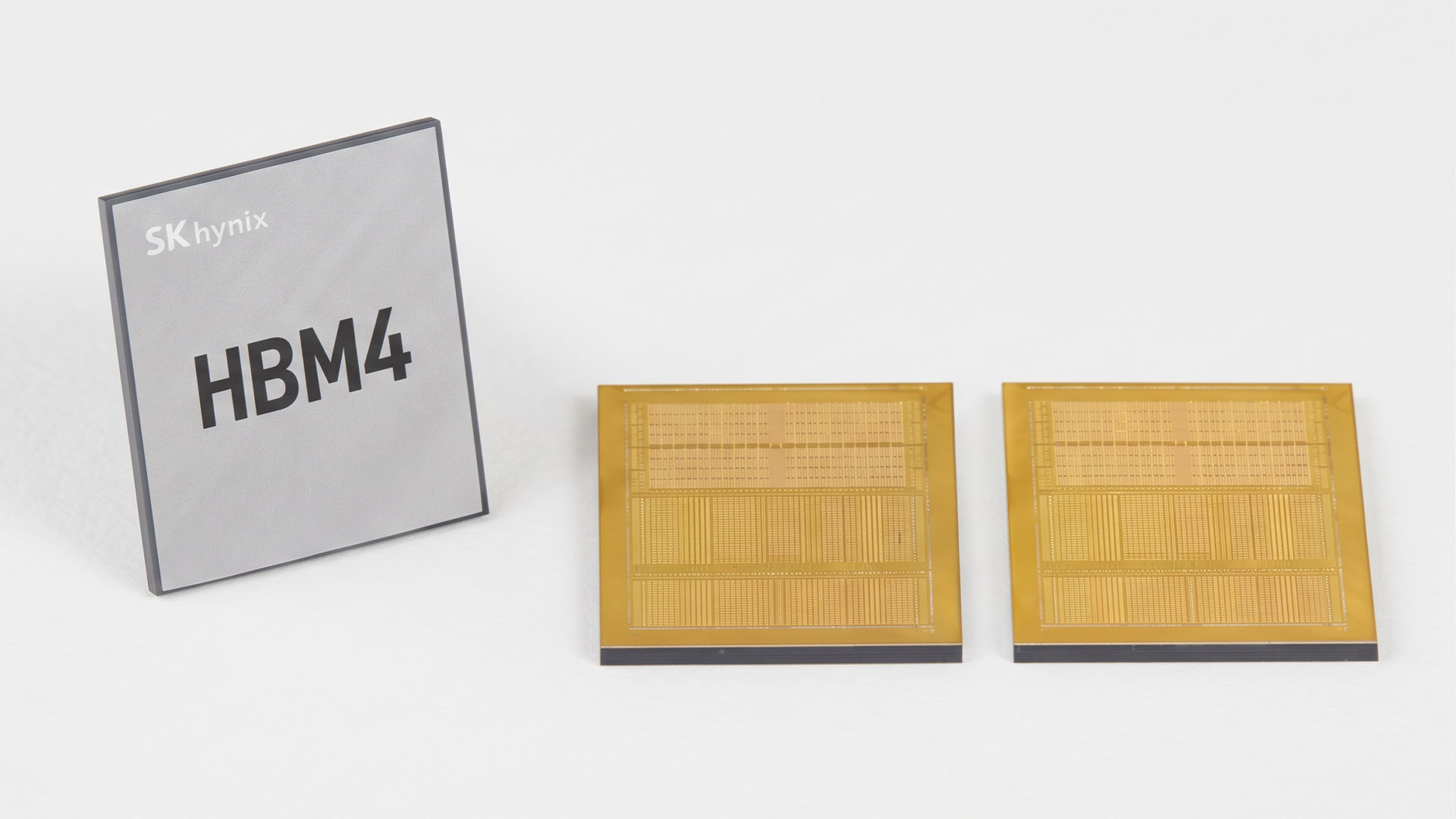
NVIDIA's NVHBM base die moves to TSMC 3nm
Samsung is checking whether its own lines can cover NVHBM base-die demand if TSMC capacity runs short, while the base die moves to TSMC's 3nm process.
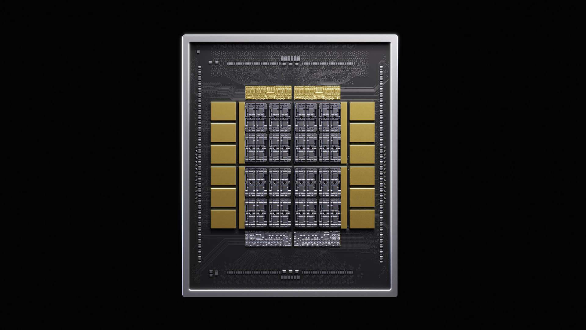
| NVHBM | |
|---|---|
| Base die process | TSMC 3nm |
| Core die process | 1c |
| Structure | HBM4E (7th-generation) |
| Memory bandwidth | up to 30% greater than HBM4E |
| HBM power | 15% lower than HBM4E |
| XPU die area | up to 25% more |
| First collaborator | Amazon Annapurna Labs |
The memory controller sits in the HBM base die.
Seoul Economic Daily says Samsung will use TSMC's 3nm process for that base die.
That node does not prove Samsung has abandoned turnkey HBM.
NVIDIA's post gives the performance case. It lists up to 30% more bandwidth, 15% lower HBM power, and up to 25% more XPU die area.
The constrained party is Samsung's foundry. The outlet says it is still checking whether its own lines can make NVHBM base dies if demand exceeds TSMC capacity.
That does not establish a permanent break.
Samsung keeps 4nm for HBM4 and HBM4E base dies, keeps turnkey for standard HBM, and keeps turnkey for AMD custom HBM.
For the buyer, one base-die process across Samsung, SK hynix, and Micron reduces separate qualification.
The packet leaves absolute bandwidth, absolute power, SKU, production start, volume, TSMC capacity, Samsung capacity, stack height, core-die count, and base-die size unmeasured.
Samsung is constrained by TSMC capacity, not by architecture, because it keeps its own foundry option open.
The 3nm base-die requirement reduces qualification work for buyers, but it does not end Samsung's turnkey HBM business.
The change is a base-die process, not a foundry break.
After m.naver.com. We did not report this. The pictures, if any, are theirs.