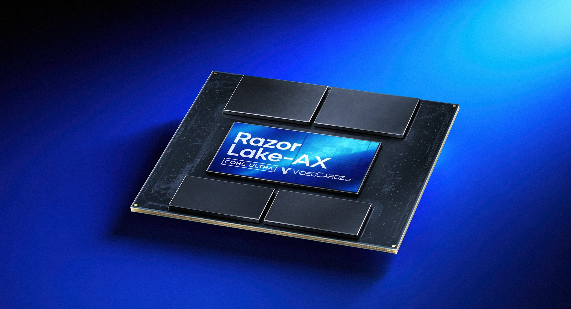
ASUS ProArt P16 pairs a 20-Core arm CPU with a 6144-CUDA blackwell die
The ASUS ProArt P16 ships with NVIDIA's N1X SoC in a 20-core, 6144-CUDA-core configuration on TSMC 3 nm, with 128 GB of unified LPDDR5X memory and a 45–80 W TDP envelope.
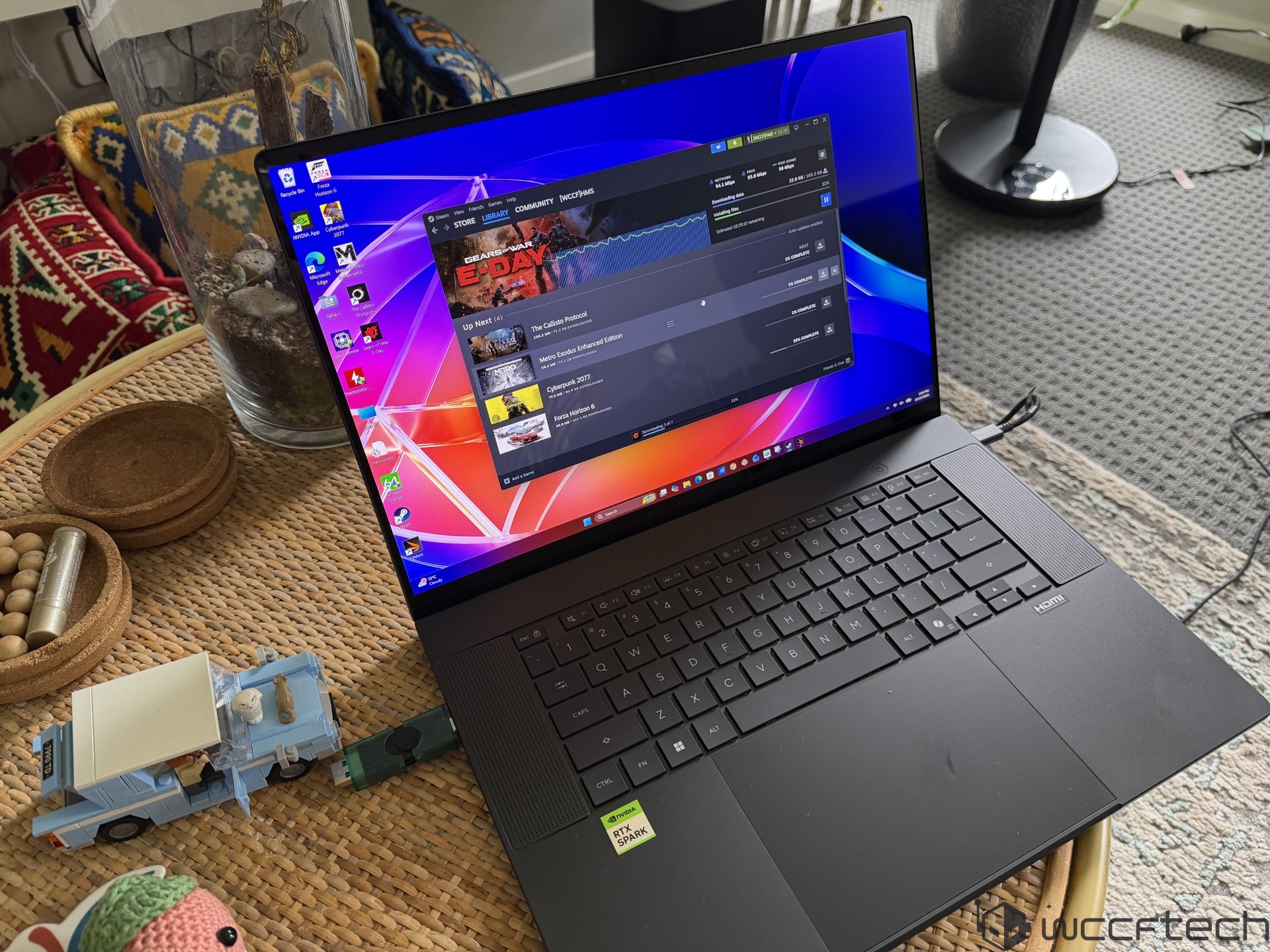
| ASUS ProArt P16 (N1X 20-core / 6144-core | |
|---|---|
| CPU cores | 20 (10 Cortex-X925 + 10 Cortex-A725) |
| GPU CUDA cores | 6144 |
| SM units | 48 |
| Memory | 128 GB LPDDR5X |
| Memory bandwidth | 300 GB/s |
| Process | TSMC 3 nm |
| TDP | 45–80 W |
| Price | TBD |
ASUS ProArt P16, price TBD, is the first retail laptop built on NVIDIA's RTX Spark platform, and the Wccftech review unit carries the N1X SoC in its fullest configuration: 20 Arm cores and a 6144-CUDA-core Blackwell GPU on TSMC 3 nm. The platform was first announced at Computex 2026, and the review unit was provided by NVIDIA during its RTX Spark Editor's Day event. The desk notes that additional benchmarks will follow as it spends more time with the device.
The N1X ships in two cuts. The lower configuration pairs 18 CPU cores (9 Cortex-X925, 9 Cortex-A725) with a 5120-CUDA-core GPU across 40 SMs at a 3.9 GHz P-core ceiling. The headline configuration adds two performance cores and 1024 CUDA cores across 48 SMs, pushing the P-core boost to 4.0–4.1 GHz while the E-core clock stays at 2.8 GHz in both.
Because the review page lists the price as TBD, the buyer cannot map a dollar figure to either cut. The stretch between the two is a 20 percent increase in CUDA cores, a 10 percent increase in CPU cores, and a step from 40 to 48 SMs. Both configurations share the same 45–80 W configurable TDP, the same 256-bit LPDDR5X memory interface, and the same TSMC 3 nm process across both dies.
The GPU's theoretical ceiling is 31 TFLOPs of FP32 and 1000 TOPS of NVFP4, which is FP4, with no sparsity multiplier stated on the spec page. The die carries 24 MB of L2 cache and fifth-generation Tensor Cores supporting DLSS, Reflex, ACE, G-Sync, CUDA, and NVFP4. The measured AI throughput in UL Procyon's text-generation suite came in at 73.81 tokens per second with a 0.37-second time-to-first-token, roughly 75 percent above the next-closest Arm laptop in the same test.
The 256-bit LPDDR5X interface runs at up to 9400 MT/s for 300 GB/s of raw bandwidth, and the unified pool tops out at 128 GB. The NVLink C2C fabric moves 600 GB/s bidirectionally between the CPU and GPU dies, with a 16 MB system-level cache sitting between them as an L4 under the CHI-E coherency protocol. The fastest discrete RTX PRO card in NVIDIA's current lineup carries 96 GB of VRAM; the N1X's unified pool exceeds that by 32 GB without a separate memory controller.
On the CPU side, the 20-core N1X posts 116 single-core and 1604 multi-core in Cinebench 2024, and 1196.6 / 15972.2 in CPU-Z, the fastest single-core score in the group. In 3DMark's CPU Profile it scores 7478 at max threads, trailing the Core Ultra X9 388H (10449) and the Ryzen AI MAX+ 395 (10385) by roughly 30 percent. The single-thread gap is smaller: 620 versus 1207 for the X9 388H, a 49 percent deficit that the 4.1 GHz boost clock does not close.
Blender renders at 156.86 samples per minute on the monster scene, ahead of the Panther Lake X9 388H (130.4) but behind the Ryzen AI MAX+ 395 (185.4). WinRAR compression lands at 17433 KB/s, mid-pack among the seven laptops tested, while AIDA64 memory bandwidth reads 120440 MB/s for reads and 211500 MB/s for writes, the fastest in the group. The Procyon Office suite scores 7166 in Word, 6810 in Excel, and 7681 in PowerPoint, trailing the X9 388H and Ryzen AI MAX+ 395 in all three.
The NVIDIA Newsroom filing on the RTX Spark platform treated the N1X as a single part number, collapsing the two configurations into one announcement. The Wccftech spec table shows two distinct cuts with different core counts, different SM counts (40 versus 48), and different P-core clocks. A buyer reading only the press release would not know that the 5120-core GPU drops two SMs and a full performance-core pair relative to the 6144-core variant.
The constraint here is not the silicon. It is the software stack. The N1X is an Arm SoC running Windows on Arm, and the Cinebench and 3DMark gaps against x86 chips are the tax that native x86 binaries pay under emulation or recompilation, a tax that no amount of cache or clock speed erases.
The 128 GB unified memory and the 600 GB/s C2C link are real architectural advantages for AI inference and large render scenes, but the 45–80 W TDP envelope means the 6144-CUDA GPU shares a power budget with 20 CPU cores in a 1.77 kg chassis. The buyer who needs sustained multi-threaded x86 workloads is constrained by the ISA, not by the die. The buyer who needs a single large model resident in memory with RTX ray tracing on the same pool is not constrained by anything in this document.
The DGX Spark, NVIDIA's desktop workstation on the same N1X silicon, is the single contrast: a fixed-form factor with a dedicated power supply versus the ProArt P16's 1.77 kg, 99.9 Wh battery chassis running at 45–80 W.
What the document does not measure is sustained GPU throughput under a 45 W cap versus an 80 W cap, thermal throttling behavior over a 30-minute render, and the retail price of either N1X configuration. The 1000 TOPS figure is a peak; the 73.81 tokens per second is a measurement. The gap between those two numbers is where the buyer's real workload will land, and no page in this packet closes it.
The N1X's 128 GB unified memory and 600 GB/s C2C link give it a structural advantage for large-model inference that no discrete GPU laptop matches. The 45–80 W envelope and the Arm ISA tax on x86 workloads mean the buyer is choosing a workload profile, not a performance tier.
Sustained GPU throughput at the 45 W cap versus the 80 W cap, thermal behavior over a 30-minute render, and the retail price of either N1X configuration.
The N1X SoC trades x86 multi-thread throughput for a 128 GB unified memory pool and a 600 GB/s NVLink C2C fabric. The 45–80 W TDP cap constrains sustained GPU performance in a 1.77 kg chassis, and the Arm ISA gap in Cinebench and 3DMark is a software-stack tax, not a silicon limitation.
After threads.com. We did not report this. The pictures, if any, are theirs. Also filed by Wccftech, NVIDIA Newsroom.