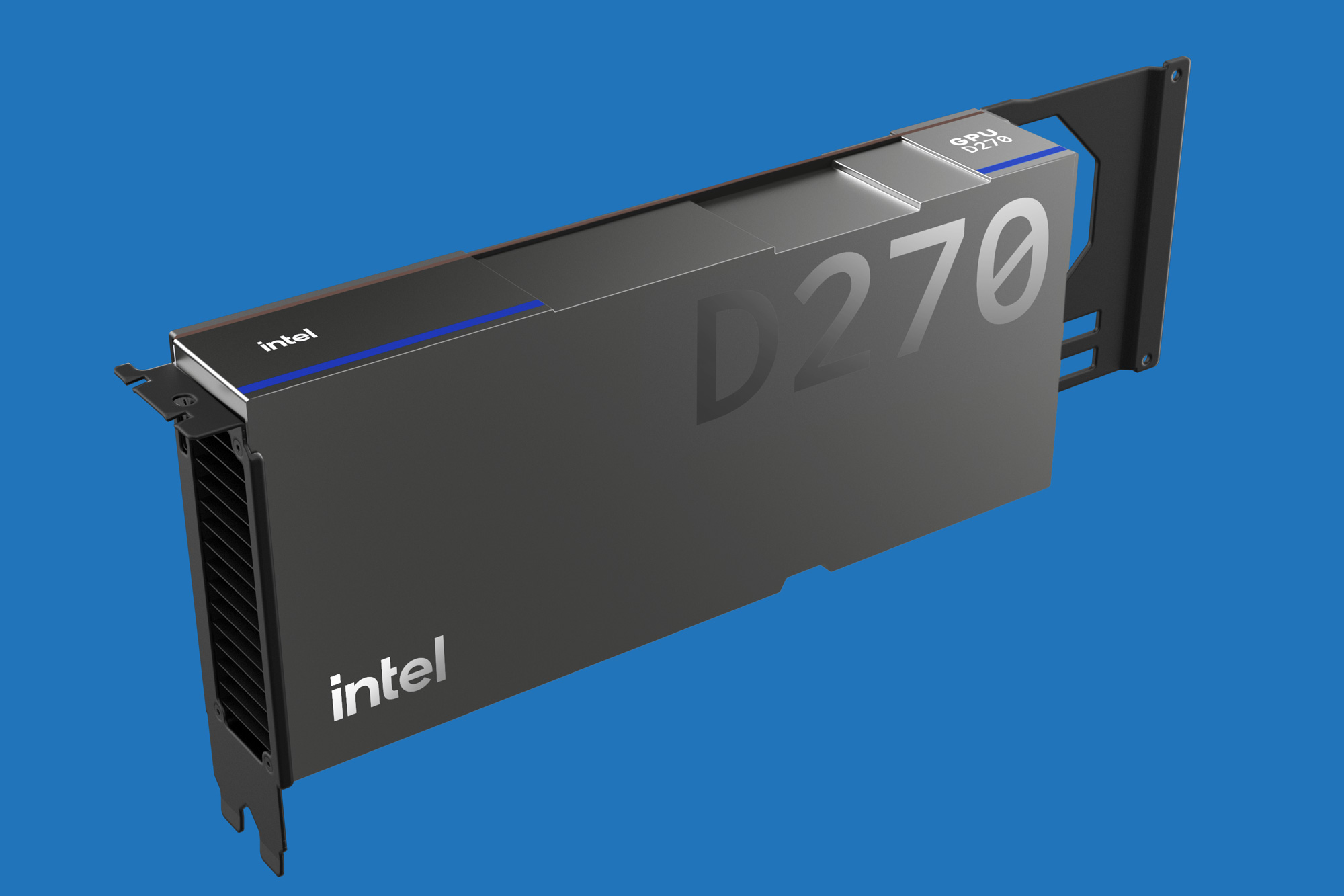
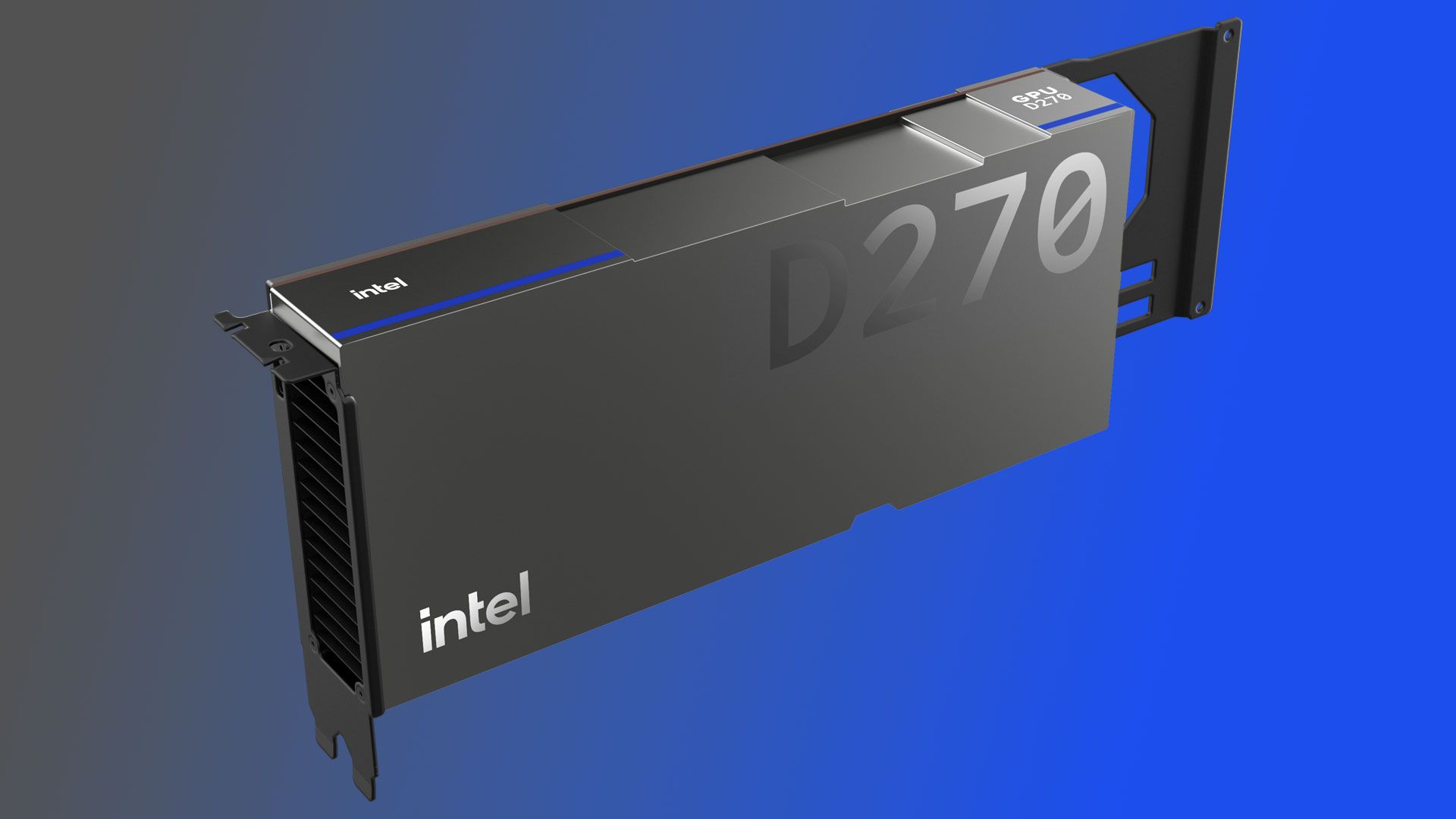
Intel GPU D270: 480 GB LPDDR5X, 32 Xe3P cores, no price
Intel's GPU D270 pairs 480 GB of LPDDR5X with 32 Xe3P cores and 256 XMX matrix engines in a 350-watt air-cooled package, but the Phoronix page of 12 October 2026 states no price.

| Intel GPU D270 | |
|---|---|
| Memory | 480 GB LPDDR5X |
| Cores | 32 Xe3P |
| Matrix engines | 256 XMX Xe3P |
| Power | 350 W air-cooled |
| Interface | PCI Express 5.0 |
The Intel GPU D270 is the flagship of the GPU D Series, the enterprise inference accelerator Intel calls Crescent Island, and the Phoronix page of 12 October 2026 names no price for it. The configuration that number describes carries 480 GB of LPDDR5X per card, 32 Xe3P cores, 256 XMX matrix engines, a 350-watt air-cooled thermal envelope, and PCI Express 5.0 connectivity. That is the entire spec sheet the vendor page offers at this stage, and it is short by the standards of a product launch that is supposed to move enterprise procurement.
The starting-price configuration is not stated anywhere in the document. The D270 is both the headline number and, as far as the page goes, the only SKU in the series.
No bandwidth number accompanies it, and the page does not state the LPDDR5X data rate in MT/s or the number of memory channels. The number sits alone, unaccompanied by a GB/s figure, a latency annotation, or a comparison to the memory subsystem of a competing card, and the reader is left to infer whether 480 GB is a theoretical peak or a sustained allocation.
Thirty-two Xe3P cores and 256 XMX matrix engines give a ratio of eight matrix engines per core. The document does not give a clock frequency, a TFLOP figure, or a sparsity multiplier, and it does not say whether the XMX engines operate at a different clock domain than the Xe3P cores. There is no FP4 claim, no structured-sparsity annotation, no "up to" qualifier on any throughput number; the architecture is named, and the peak is not.
The page says the series is "geared for agentic AI," which is a workload description, not a specification. It implies long context windows, sustained memory pressure, and a compute pattern more sequential than the batched matrix multiply of a training run. The 480 GB envelope makes sense for that pattern, but the page does not state a maximum context length, a token-per-second figure, or a concurrency number, and the agentic framing remains a marketing position rather than a measured capability.
The term "inference-optimized" in the page's description of the D Series is a design intent, not a measured result. It suggests the Xe3P cores and XMX engines are tuned for the latency-sensitive, memory-bandwidth-bound pattern of serving a model at a fixed batch size, rather than the throughput-optimized pattern of training. The 480 GB of LPDDR5X supports that reading, because a large on-card memory pool reduces the need to offload weights to system RAM or to a separate memory tier, but the page does not benchmark the card against a serving workload and the optimization claim is unverified.
Three hundred and fifty watts, air-cooled, on a PCI Express 5.0 slot. The document does not state the card's physical dimensions, its slot width, or whether it is a single-slot or dual-slot design, and it does not say whether the 350-watt figure is a TDP, a TBP, or a maximum sustained draw under a defined workload. A 350-watt air-cooled envelope on PCIe 5.0 is a constraint the data-center buyer will test against rack density, chassis airflow, and PSU headroom before the first unit arrives in a chassis, and the form-factor question is left open.
The PCI Express 5.0 connection is the interface claim, and it is the one figure that tells the buyer something about the card's role in a multi-GPU node. PCIe 5.0 x16 delivers a theoretical 64 GB/s in each direction, which is enough to keep the 480 GB memory subsystem fed under a single-stream workload. The page does not state the lane count, and it does not say whether the card supports a multi-card interconnect for scaling beyond a single PCIe slot.
The Linux driver path is the one forward-looking claim in the page. Larabel writes that upstream support "has been coming along well" and should be in place "by the time these accelerators are shipping at scale." No kernel version is named, no driver version is pinned, and the Phoronix sidebar references Linux 7.4 in unrelated articles without tying the Crescent Island driver to a specific release or a specific feature set.
The packet contains no competing desk's error to correct. No Wccftech or VideoCardz headline in the dossier misstates a figure or collapses a distinction that the Phoronix page preserves.

The buyer of this card is constrained by the absence of a price, a launch date, and a single measured benchmark. The 480 GB of LPDDR5X is a capacity claim, not a throughput claim, and the 32 Xe3P cores are a count, not a performance figure. Intel has named the architecture and the memory envelope, but the fab-level question—what the Xe3P core delivers per watt at inference workloads, what the XMX engine does at FP8 versus FP16, what the LPDDR5X bus sustains under a long-context agentic workload—remains outside the document. The buyer who needs a number for a TCO spreadsheet has nothing to put there, and the fab that must qualify the silicon for a data-center deployment has no thermal curve or power envelope to work from.
NVIDIA's current inference lineup pairs HBM with a different memory hierarchy, and the 480 GB LPDDR5X figure is a different bet on where inference memory lives.
What is still unmeasured: memory bandwidth, sustained compute throughput, power draw under load, physical dimensions, form factor, a specific driver or kernel version, a launch date, a price, and any benchmark result. The document names the machine. It does not measure it.
The D270 is a capacity and architecture announcement, not a performance announcement, and the buyer who needs a throughput number or a price to justify a procurement cycle has nothing in the document to work from. The 480 GB LPDDR5X envelope is a bet on on-card memory for agentic inference, but without a bandwidth figure or a benchmark, the bet is unpriced and unverified.
Memory bandwidth, sustained compute throughput, power draw under load, physical dimensions, form factor, a specific driver or kernel version, a launch date, a price, and any benchmark result are absent from the document.
The D270 spec sheet gives a memory capacity (480 GB LPDDR5X), a core count (32 Xe3P), a matrix-engine count (256 XMX), a thermal envelope (350 W air-cooled), and an interface (PCIe 5.0). It does not give a clock, a TFLOP figure, a bandwidth number, a price, a launch date, or a benchmark. The 8:1 XMX-to-core ratio is the only architectural ratio stated. The buyer cannot compute a cost-per-token or a watts-per-token from this document.
After paypal.com. We did not report this. The pictures, if any, are theirs. Also filed by SemiAnalysis-adjacent HN.