AMD MI455X carries 432 GB of HBM4 and no published price
AMD's MI455X spec page lists 432 GB of HBM4, a 40.3 PFLOPs OCP MXFP4 peak, and a 7/23/2026 launch date, but no price, no TDP, and no rack configuration.
| AMD Instinct MI455X | |
|---|---|
| Architecture | CDNA5 |
| Lithography | TSMC 2nm | 3nm FinFET |
| Work Group Processors | 256 |
| Peak Engine Clock | 2400 MHz |
| Memory | 432 GB HBM4 |
| Memory Bandwidth | 23.3 TB/s |
| Peak OCP MXFP4 | 40.3 PFLOPs |
| Launch Date | 7/23/2026 |
AMD's product page for the Instinct MI455X, the specific SKU inside the MI400 family, lists a 432 GB HBM4 accelerator on the fifth-generation CDNA architecture, with a launch date of 7/23/2026 and no price printed anywhere on the sheet. The page is the HTML specification page at amd.com, and it is the deepest document in this packet. The brochure PDF that sits alongside it carries the same numbers in a different layout, but the spec page is where the grid lives.
The headline figure is 40.3 PFLOPs, and it is a theoretical peak for OCP MXFP4, not a measured throughput from a running model. The same section on the page lists 20.1 PFLOPs for OCP MXFP6, OCP MXFP8, and FP8, all as peaks. Matrix FP16 peaks at 5 PFLOPs dense and 10.1 PFLOPs with structured sparsity, which is a 2:1 pattern applied to the matrix units. The sparsity number is a silicon capability, not a workload result. Vector FP16 and FP32 both peak at 315 TFLOPs, and FP64 peaks at 5 TFLOPs for both matrix and vector paths. No measurement, no benchmark, no third-party number appears on the page.
The document does not define a starting configuration or a base SKU. There is one die, one memory size, one clock. The 432 GB of HBM4 across 12 stacks at 23.3 TB/s is the only memory configuration listed, and the 40.3 PFLOPs MXFP4 peak describes that same single die at 2400 MHz on 256 work group processors. There is no lower-tier trim, no reduced-memory variant, no price tier. The stretch between a base and a headline does not exist because AMD published one configuration and one number. The 192 MB L2 cache and the ECC support are fixed, not configurable.
The Spheron blog post that triggered this filing carries the title "AMD MI400 vs NVIDIA B300: MI455X Specs, Price (2026)." The word "Price" in that headline has no referent in the AMD document. The AMD page names its comparison target "NVIDIA Vera Rubin," not "B300," which is a different product designation. The Spheron title also collapses the MI400 family name with the MI455X SKU, which is a small error but one that makes it unclear which die the specs describe.
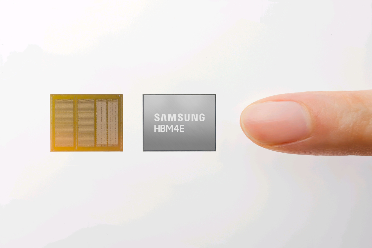
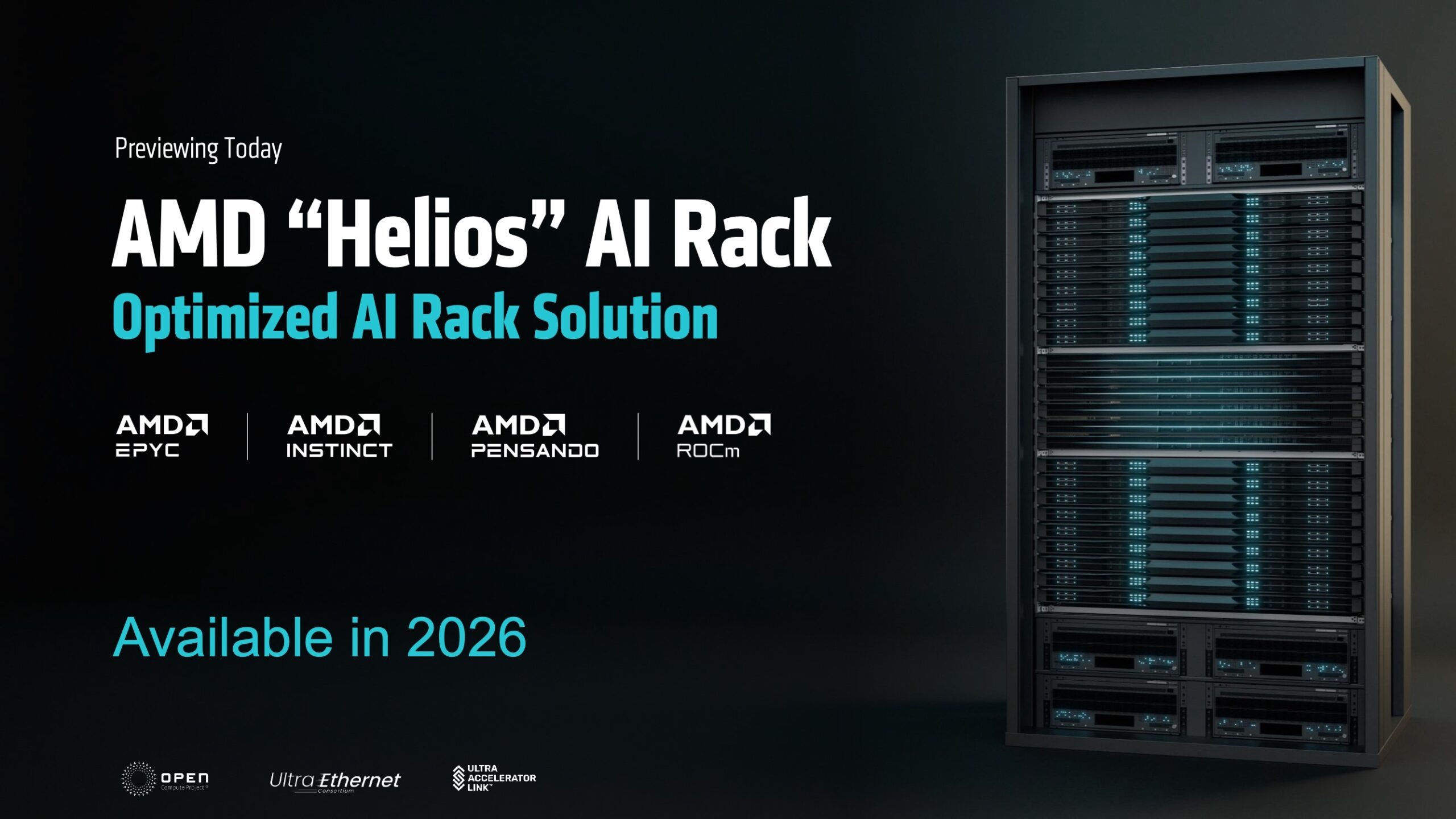
The 320 billion transistors sit on a TSMC 2nm and 3nm FinFET process, a two-node design in a single package. The EAM form factor and direct liquid cooling mean this is not a card you slot into a workstation. It is a module built for the Helios rack-scale system, which AMD describes as combining Instinct GPUs, EPYC server CPUs, and Pensando networking. The 3.6 TB/s UALoE scale-up bandwidth determines how many of these GPUs can exchange data inside a single rack before the interconnect becomes the bottleneck, and the 600 GB/s UALink scale-out bandwidth determines how racks talk to each other. Both are peak figures, not sustained figures.
The software list on the page runs through OpenMP, OpenCL, HIP, ROCm, TensorFlow, PyTorch, ONYX-RT, SGLang, JAX, Triton, Kokkos, and RAJA. The OS support is Linux x86 64-bit only, which is a datacenter constraint, not a consumer one. The ROCm ecosystem has been AMD's answer to CUDA since 2016, and the MI455X does not change that relationship.
The 12 stacks of HBM4 at 23.3 TB/s is the memory architecture that matters for inference workloads. Each stack works out to 36 GB, which is the standard HBM4 stack size. The 192 MB L2 cache sits between the 256 work group processors and the memory controller, and the ECC support is a datacenter requirement rather than a consumer feature. The memory bandwidth number is the one that separates this die from the previous generation, and it is the number a model architect checks first.
The buyer is constrained by three absences: no price, no TDP, no per-rack GPU count. AMD published the silicon specification but not the commercial terms. A datacenter operator cannot model a rack's power draw, cannot calculate a per-token inference cost, and cannot confirm whether the Helios rack holds eight, sixteen, or thirty-two MI455X units. The 40.3 PFLOPs number is a ceiling calculated by AMD Performance Labs in June 2026, per the footnote on the page, and the gap between that ceiling and what a sustained inference workload actually sustains is the number that drives a capex decision. AMD has not published that gap, and no third party has measured it.
For contrast, the same AMD page lists NVIDIA Vera Rubin at 288 GB of memory and 22.0 TB/s of bandwidth, which puts the MI455X ahead on both figures by a margin that is real but narrow.
What the page left out: the price, the thermal design power, the number of GPUs per Helios rack, and any measured benchmark. The MXFP4 peak is a theoretical calculation, not a measurement. The buyer still cannot know what the MI455X sustains under a long inference load, what the Helios rack's aggregate power envelope is, or what the per-unit cost is at volume. The 7/23/2026 date is a launch date, not a shipping date, and the document does not say whether that date marks a press event, a first shipment, or an order-open.
The buyer cannot model a rack's power draw or a per-token cost because AMD published the silicon spec without the commercial terms. The 40.3 PFLOPs ceiling is a June 2026 AMD Performance Labs calculation, and the gap between that ceiling and sustained inference throughput is the number a capex decision actually needs.
The document does not state a price, a TDP, a per-rack GPU count, or a measured benchmark.
The MI455X spec is complete on the silicon side and absent on the commercial side. No TDP, no price, no per-rack GPU count means a datacenter operator cannot build a power model or a cost model from this document alone. The 40.3 PFLOPs MXFP4 peak is a theoretical ceiling, not a measurement, and the structured sparsity figures (10.1 PFLOPs FP16, 10.1 POPs INT8) are silicon capabilities that do not reflect what a real model sustains.
After amd.com. We did not report this. The pictures, if any, are theirs. Also filed by spheron.network, rtx50series.co.uk.