Foveros stacking gives the note a shape, but the date decides it
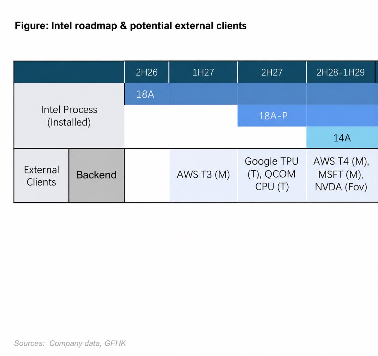
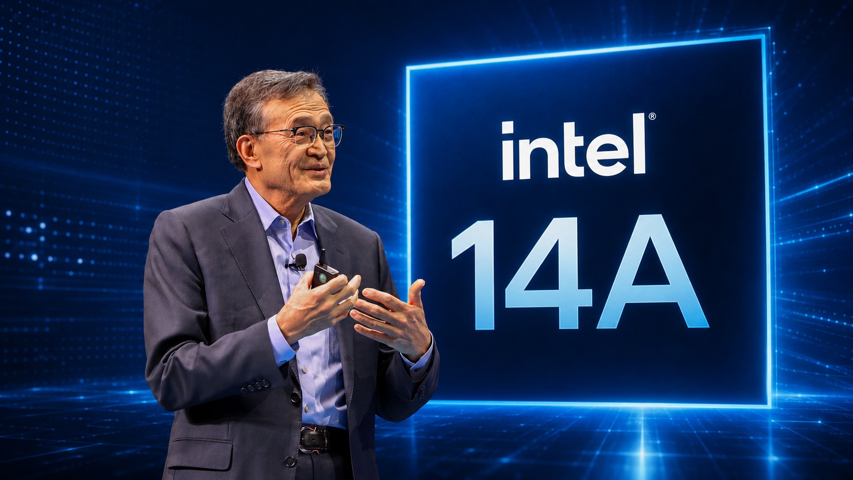
H2 2028 is the fact that turns the Foveros note into a possible NVIDIA backend question, because Intel 14A is expected to enter production then.
| Foveros | EMIB-T | |
|---|---|---|
| stacking | 3D stacking | horizontal placement |
| customer tip | NVIDIA might also use | Google's interest for TPU AI chips |
| 14A production | H2 2028 | |
| TSV | integrates TSVs into bridge |
The Wccftech page frames the 14A production date as a possible backend window for NVIDIA, while Jeff Pu's X post only mentions external backend customers. Those two descriptions do not line up, and the page that carries the window is the one that matters for the timeline.
Foveros is described as true 3D stacking, with computing tiles placed on a base die rather than arranged horizontally as in EMIB. That geometry is the only architectural reason the note has weight now. It suggests a smaller package footprint and better power and data paths, but the page supplies no measured difference.
The buyer sees a possible second packaging source, not a confirmed one. The note does not prove a contract, a volume, or a model. If the H2 2028 window holds, TSMC packaging pressure may ease, and Intel's backend becomes a real option for non-core IP. The fab gains a customer story; the buyer gains a schedule risk.
No page measured Foveros power, data speed, yield, or NVIDIA adoption. The note leaves out contract value, production volume, and a confirmed backend customer. Until those numbers appear, the claim is a date, not a design for the buyer and the fab today.
Intel is constrained by proof, not by concept. The note gives a date, not a contract, so the buyer should treat Foveros as a schedule option, not a confirmed backend.
After x.com. We did not report this. The pictures, if any, are theirs.