M6 on N2: twelve GPU cores, doubled NPU, same 128-bit bus
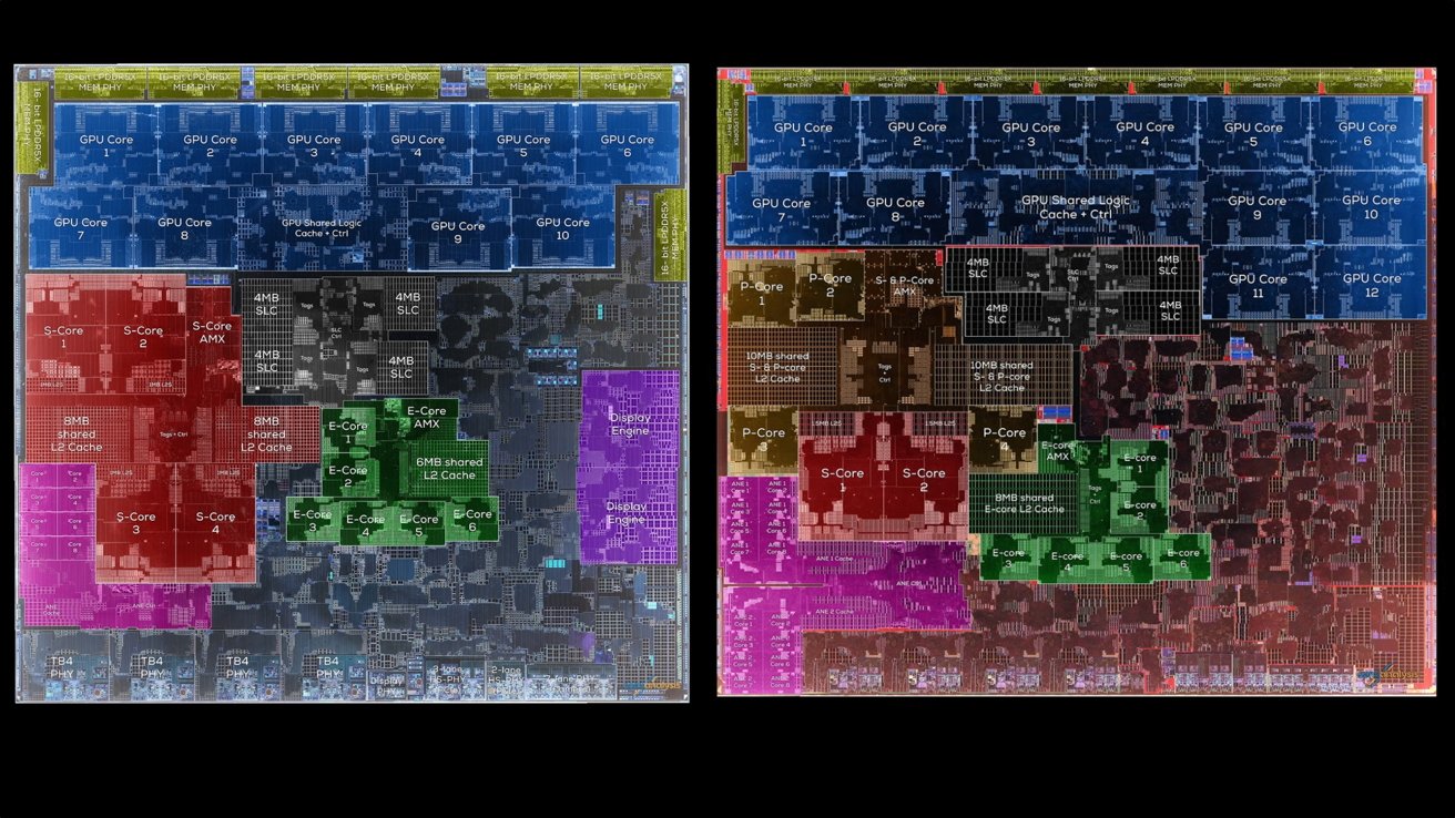
High Yield compares M6 and M5 die shots from SemiAnalysis STEEL; the M6 adds two GPU cores, a dual NPU, and six unified PCIe lanes on TSMC N2.
| Apple M5 | Apple M6 | |
|---|---|---|
| Process | N3P | N2 |
| Die size | 154 mm² | 141.6 mm² |
| GPU cores | 10 | 12 |
| Memory bandwidth | 153.6 GB/s | 153.6 GB/s (16 GB) / 170 GB/s (24/32 GB) |
| SLC | 16 MB | 16 MB |
| CPU | 4 S + 6 E | 2 S + 4 P + 6 E |
| S-core L2 | 1 MB private | 1.5 MB private |
| Shared L2 | 16 MB, S-cores | 20 MB, S- and P-cores |
| E-core cache | 6 MB | 8 MB |
| NPU | 16-core | dual 16-core |
| PCIe | 3× gen4 + 2× gen3 | 6× gen4 |
The M6 is the first desktop-class Apple SoC fabricated on TSMC's N2 node, and High Yield walks through die shots of both the M6 and the M5, both captured by the STEEL team at SemiAnalysis. The M6 measures 12.8 by 11.06 millimeters, 141.6 square millimeters, about 8 percent smaller than the M5's 12.75 by 12.08 millimeters and 154 square millimeters on N3P. The memory interface sits on the top shoreline of both dies: eight 16-bit LPDDR5X PHYs, a 128-bit bus.
Under that shoreline the GPU goes from ten cores to twelve, the first core-count increase since the M2, and each M6 core is over 10 percent smaller. Below the GPU, the system-level cache is 16 MB on both chips, four SRAM blocks of 4 MB. The M5 had already doubled that cache from the M4's 8 MB.
The CPU floorplan is the break with the M5. That die has four S-cores, each with a 1 MB private L2 slice, set around 16 MB of shared L2 in two 8 MB blocks, and a separate cluster of six E-cores around 6 MB. The M6 keeps two large S-cores and raises the private slice to 1.5 MB, half again the M5 slice. Those S-cores are smaller than the M5's even with the larger private cache. The two S-cores and four new P-cores share two 10 MB blocks, 20 MB in all, 4 MB more than the M5, and High Yield reads the left block as an 80 KB SRAM macro. The P-cores come in under half the area of an S-core, which is why he says Apple calls them M-cores internally. The E-core cluster stays separate: six cores around 8 MB of shared cache, 2 MB more than the M5, with its own AMX. The S- and P-cores look to share one AMX between them.
The neural engine doubles beside that cluster. The M5 draws its 16-core ANE as eight dual-cores plus a local cache. The M6 places two clusters side by side, eight dual-cores and a cache on each, meeting in one control area. He calls that dual 16-core block more symmetrical than the A20 Pro. Two display engines sit on the right edge of both dies. Along the bottom, the four-lane display PHY and the seven-lane camera PHY match the M5. High Yield reads the M5 high-speed lanes as three PCIe gen4 plus two smaller gen3, and the M6 as six lanes of one design, the same lane used in the Thunderbolt PHYs, which he takes as gen4. He counts the same Thunderbolt 4 ports on the M6, and treats Thunderbolt 5 as a Pro-chip part.
A die shot shows placement and area. Clocks, power, and a measured gain from four P-cores in place of two S-cores sit outside the frame. Unmarked silicon holds the media engine, encode and decode, audio, and the rest of a SoC, and he leaves those blocks unlabeled because the names would be guesswork.
Twelve GPU cores at 9,600 MT/s on that 128-bit bus is the same 153.6 GB/s the M5 delivered with ten cores. The 16 GB M6 uses the same DRAM. The 24 GB and 32 GB M6 parts reach 170 GB/s on 10,667 MT/s DRAM. Every base M-series chip since the M1 has used this width. High Yield expects an M7 to widen it, and he points at the 96-bit buses on the A20 and A20 Pro as the hint.
N2 density buys area headroom, but the DRAM path is unchanged since M1. The P-core swap is an area trade, not a proven performance win, absent clock and thermal data.
After High Yield. We did not report this. The pictures, if any, are theirs.