AMD 5900X3D engineering sample shows 128MB asymmetric L3
An unreleased 12-core AM4 engineering sample reports 128MB of L3, with 96MB on one CCD and 32MB on the other.
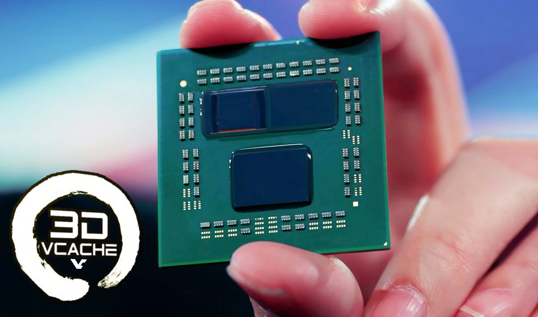
The engineering sample reports 128MB of L3 cache. It is a 12-core AM4 part, with one CCD carrying 96MB and the other 32MB. VideoCardz places the 128MB measurement inside the 192MB upper limit, between the standard 5900X layout and both-CCD lab prototypes. A 64MB V-Cache die sits above one CCD, raising that chiplet from 32MB to 96MB.
Buyers are constrained by absence, not by cache size. AMD tested the 128MB asymmetric layout, but the document does not prove it was ready for retail, and no Ryzen 5000 desktop part shipped with that total. Performance remains unproven, so the buyer cannot infer game, workload, or thermal gain from cache alone. For the fab, the sample marks a test point between 64MB and 192MB, not a missing SKU.
Load, power, temperature, benchmark, price, and availability are not measured. BIOS support is measured only as boot behavior: latest BIOS stops at error code 90, older SMU firmware 56.70.0 reportedly works. Chiphell owner contacted ASRock about adding support to a newer BIOS. That gap still leaves the part outside the released Ryzen 5000 desktop lineup for now.
The buyer is constrained by absence, not by cache size. The sample is a fab test point between 64MB and 192MB, not a missing retail SKU.
The 128MB layout proves one-CCD V-Cache stacking was tested on a 12-core AM4 part, but it does not establish performance, power, or retail readiness.
128MB total L3 cache · 12-core AM4 processor · 96MB on V-Cache CCD · 32MB on second CCD · 192MB both-CCD prototypes · SMU firmware 56.70.0
After videocardz.com. We did not report this. The pictures, if any, are theirs.